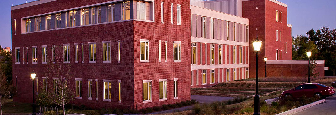
Characterization
The Characterization Facility offers world-class analytical services to the University of Arkansas, with cutting-edge capabilities in high-resolution imaging, spectroscopy, and sample preparation that support advanced materials research.
Materials Institute Cleanroom
The Materials Institute Cleanroom is a state-of-the-art fabrication facility supporting advanced research, education, and innovation in semiconductor processing, device fabrication and related technologies. The cleanroom provides an ISO 5 / Class 100 controlled environment with industry-standard contamination control protocols, enabling reliable fabrication, characterization, and integration of advanced micro- and nanoscale devices.
Affiliated Facilities
Molecular Beam Epitaxy (MBE)
The molecular beam epitaxy (MBE) is a highly controlled thin-film deposition technique used to grow crystalline materials one atomic layer at a time. MBE enables precise control over film thickness, composition, and interfaces, making it ideal for fabricating high purity advanced semiconductor devices and quantum structures.
MonArk NSF Quantum Foundry
The MonArk NSF Quantum Foundry is an NSF program that is jointly led by Montana State University and the University of Arkansas with the overarching mission to use robots and AI to accelerate two-dimensional materials research for quantum technologies in the US.
The Institute for Integrative & Innovative Research (I3R)
The I3R is a new kind of public research institute, one with convergence at its core and differentiated by a dual mandate to advance research excellence and impact economic development.
High-Density Electronics Center (HiDEC)
The HiDEC is a core R&D facility that provides the tools, education and expertise to enable ground-breaking electronics research, prototyping and fabrication.
National Multi-User Silicon Carbide Research Fab (MUSiC)
The National Multi-User Silicon Carbide Research Fab is the only low volume SiC integrated circuit fabrication facility to develop breakthroughs in the semiconductor area.